
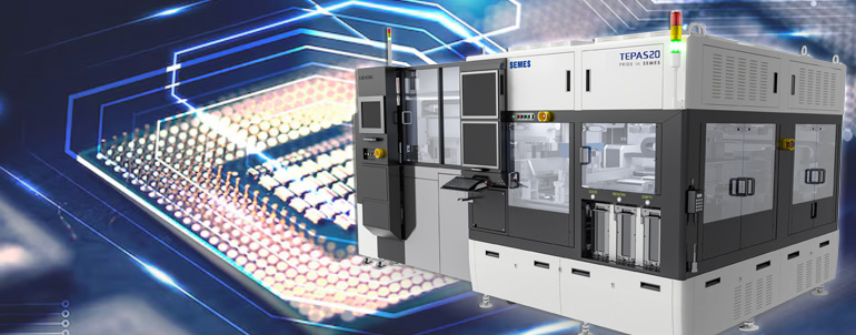
Next-Generation Sorter for Advanced Panel-Level Packaging (PLP)
The SEMES TEPAS100 is the semiconductor industry’s premier, high-speed, high-precision sorter engineered specifically for large-format Panel-Level Packaging (PLP) production lines. As advanced packaging scales to meet the massive demands of AI, high-performance computing (HPC), and dense chip integration, the TEPAS100 delivers an all-in-one automated solution for the final, critical stages of back-end processing.
Core System Workflow
The TEPAS100 seamlessly unifies multiple post-singulation processes into a single, optimized inline system:
Singulation Handling
Panel ExtractionDices and safely extracts singulated package chips directly from massive 515mm x 510mm panels.
Proprietary Cleaning & Drying
Tornado Blower TechnologyUtilizes an exclusive, wide-area Tornado Blower method to achieve high-speed, uniform drying across large panel surfaces immediately after singulation, eliminating moisture and residual debris.
Vision Inspection
Defect ClassificationEmploys high-resolution, ultra-fast vision inspection systems to dynamically differentiate known-good-die (KGD) from defects.
Precision Sorting
Tray PlacementSorts and transfers passing chips into high-density shipping or testing trays using rapid, high-accuracy pick-and-place robotics.
Key Technical Advantages
Discover the performance optimizations built directly into the SEMES PLP structural pipeline:
Large Panel Capability
Purpose-built to handle ultra-large 515mm x 510mm panels, unlocking the full throughput advantages of PLP over legacy wafer-level packaging.
Superior Defect & Quality Control
Advanced machine vision ensures absolute accuracy in defect screening, protecting your downstream supply chain and maintaining flawless yield metrics.
Differentiated Productivity
The specialized Tornado Blower drying system dramatically slashes cycle times per panel, preventing the cleaning phase from becoming a throughput bottleneck.
Versatile Packaging Roadmap
Engineered to scale seamlessly from legacy packaging formats up to highly integrated, ultra-thin advanced PLP architectures.
Our Semiconductor and PCB Films
Various Application and Customizations

Singulation Tape
Secures Chips During cutting; Offers precise UV release.

Backgrinding Film
Supports wafers during thinning; prevents breakage.

Heat Release Film
Supports package dicing; prevents breakage and residue Free.

Toyo Adtec Precision Pre-Cut Dicing Films
Zero Airborne Contam and Perfect Frame Alignment Fit to customer needs.

Backgrind Tapes
Supports wafers during thinning; prevents breakage.

Polyimide Film
Paired with high-performance silicone or acrylic adhesives, it peels away perfectly clean after processing.

Mylar Carrier Film
The ceramic dielectric slurry is coated directly onto the moving PET film via a doctor blade or die coater.

Die Attach Film
Die Attach Film is adhesive film which is used for semiconductor process environments.